Faculty

Hugh Roy and Lillie Cranz Cullen Distinguished University Chair
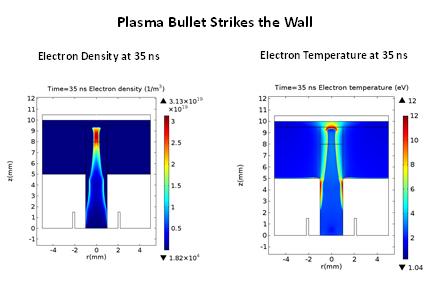
LOW TEMPERATURE ATMOSPHERIC PRESSURE PLASMAS
Interest in low-temperature atmospheric-pressure plasmas is fueled to a large extent by realized and potential biomedical applications. For selected area exposure, so-called atmospheric pressure plasma jets (APPJ) are most common. The plasma generated by this source extends up to several cm from the end of the tube where it mixes with open air, making it ideal for treating specimens, including bacteria-covered surfaces, or living tissue. Although the jet appears to be continuous, it consists of periodic streamers or “bullets” that propagate at speeds of 10 km/s or more. A typical setup is shown in the figure below. We are employing plasma transport and reaction models to predict the spatiotemporal profiles of plasma species and electric field in the system. The physics of bullet interaction with specimens is of particular interest. The fluxes of important species (e.g., O atoms and ozone in the case of He plasma gas in an O2 ambient) on the surface of the specimen are predicted for both insulating and conducting surfaces, and compared to data.
An atmospheric pressure plasma jet impinging on a quartz substrate.
ELECTROMAGNETIC WAVE-PLASMA INTERACTIONS IN VERY-HIGH FREQUENCY CAPACITIVELY COUPLED PLASMA REACTORS
The objective of this project is the fundamental understanding of how electromagnetic (EM) waves interact with capacitively coupled plasma (CCP) discharges, driven at very high frequency (VHF ~10s-100s MHz). This topic is highlighted in the 2016 Department of Energy Report of the Panel on Frontiers of Plasma Science. CCP discharges have emerged as the workhorse technology in a wide variety of applications, including fabrication of nano-devices with very stringent requirements. CCP discharges are traditionally electrostatically driven, but recent VHF operation has magnified the importance of the physics of coupling of electromagnetic waves with the plasma. Such coupling is still poorly understood despite nearly two decades of research in this area. This is mainly due to the scarcity of space- and time-resolved experimental measurements of key variables, and unresolved physics representation in computational models of VHF-CCP discharges.
2011-2014: Editorial Board, Journal of Applied Physics & Applied Physics Letters.
2011: W. T. Kittinger Teaching Excellence Award (Highest teaching honor of the College of Engineering)
2010-present: Hugh Roy and Lillie Cranz Cullen Distinguished University Chair
2009: Esther Farfel Award (Highest honor accorded to a UH faculty member)
2008: Plasma Prize, Plasma Science and Technology Division, American Vacuum Society
2008: Fluor Daniel Faculty Excellence Award, College of Engineering, University of Houston (Highest Award of the College of Engineering)
2008: Senior Faculty Award for Excellence in Research and Scholarship, University of Houston (Highest research award of the University of Houston)
2003: Fellow, American Vacuum Society
2003: Outstanding Teaching Award, Cullen College of Engineering, University of Houston
2002: Sigma Xi Faculty Research Award
Guest Editor: IEEE Trans. Plasma Science, Special Issues, August 1995, October 1999, August 2003 and October 2007
Guest Editor: Thin Solid Films, Special Issues, 2000, 2007
1998-present: International Editorial Board, Materials Science in Semiconductor Processing
1999: Senior Faculty Research Excellence Award, College of Engineering, University of Houston
1996-2010: John and Rebecca Moores Professor
1995: Excellence in Research and Scholarship Award, University of Houston
1992: Best Young Author Paper Award of the Journal of Electrochemical Society
1991: Young Faculty Research Excellence Award, Cullen College of Engineering, University of Houston
- U.S. Patent #7,883,839 “Method and Apparatus for Nanopantography,” with V. Donnelly, P. Ruchhoeft, L. Xu; S. C. Vemula; and M. Jain.
- U.S. Patent #10,515,782 “Atomic Layer Etching with Pulsed Plasmas,” Taiwan Patent No.1567819, Japan Patent No. 5826746, Japan Divisional Patent No. 593838, with V. Donnelly.
- U.S. Patent #4,859,277 “Method for Measuring Plasma Properties in Semiconductor Processing,” with G. Barna.
- U.S. Patent #8,968,588 “Low Electron Temperature Microwave Surface-Wave Plasma (SWP) Processing Method and Apparatus,” with Jianping Zhao, Lee Chen, Vincent M. Donnelly, Merritt Funk and Radha Sundararajan.
- “Systems and Methods for Rapidly Fabricating Nanopatterns in a Parallel Fashion Over Large Areas,” U.S. Patent App. 15/534,312, 2017; International Publication Number WO 2016/094353 A1, with V. M. Donnelly and S. Tian.
- U.S. Patent #7,358,484 “Hyperthermal Neutral Beam Source and Method for Operating,” with L. Chen and V. Donnelly.
- U.S. Patent #9,852,893 “Dipole Ring Magnet Assisted Microwave Radial Line Slot Antenna Plasma Processing Method and Apparatus,” with Lee Chen, Jianping Zhao and Merritt Funk.
Journal Papers / Refereed Journal Publications
- L. F. Du, D. J. Economou, and V. M. Donnelly, “In-plasma Photo-Assisted Etching of Si With Chlorine Aided by an External Vacuum Ultraviolet Source,” J. Vac. Sci. Technol. B, 40, 022207, doi.org/10.1116/6.0001710. Special topic collection on Plasma Processing for Advanced Microelectronics. This article was selected a JVST Editor’s Pick., 2022
Link to file - L. F. Du, P. Ruchhoeft, D. J. Economou, and V. M. Donnelly, “Absolute Measurement of Vacuum Ultraviolet Photon Flux in an Inductively Coupled Plasma Using a Au Thin Film,” J. Vac. Sci. Technol. B, 40, 022206, doi.org/10.1116/6.0001709. Special topic collection on Plasma Processing for Advanced Microelectronics, 2022
Link to file - T. Nguyen, P. Lin, D. J. Economou and V. M. Donnelly, “Optical Emission Self-Actinometry for Measuring Absolute Number Densities of Air Species Diffusing Into a Helium Atmospheric Pressure Plasma Jet,” J. Phys. D: Appl. Phys, 54, 405203, doi.org/10.1088/1361-6463/ac10a2, 2021
Link to file - P. Lin, J. Zhang, T. Nguyen, V. M. Donnelly and D. J. Economou, “Simulation of an Atmospheric Pressure Plasma Jet with Coaxial Shielding Gas,” J. Phys. D: Appl. Phys. 54 075205 (16pp), doi.org/10.1088/1361-6463/abc2f1 , 2021
Link to file - J. Zhang, Y. Wang, D. Wang and D. J. Economou, “Numerical Simulation of Streamer Evolution in Surface Dielectric Barrier Discharge With Electrode-Array.” J. Appl. Phys. 128, 903301-1 to 903301-13, doi.org/10.1063/5.0013594 , 2020
Link to file - L. F. Du, E. W. Hirsch, V. M. Donnelly and D. J. Economou, “Effects of O2 Addition on In-Plasma Photo-Assisted Etching of Si With Chlorine.” J. Vac. Sci. Technol. A 38, 053003-1 to 053003-8, 2020, doi.org/10.1116/6.0000338 [Invited paper in special issue commemorating J. Coburn]., 2020
Link to file - K. Zhao, D.-Q. Wen, Y.-X. Liu, M. A. Lieberman, D. J. Economou, and Y.-N. Wang, “Observation of Nonlinear Standing Waves Excited by Plasma Series Resonance-Enhanced Harmonics in Capacitive Discharges,” Phys. Rev. Lett. 122, 185002-1 to 185002-5, doi.org10.1103/PhysRevLett.122.185002, 2019
Link to file - K. Zhao, Y.-X. Liu, D.-Q. Wen, D. J. Economou, and Y.-N. Wang, “A New B-dot Probe Circuit for Magnetic Diagnostics of Radio Frequency Discharges,” Review of Scientific Instruments 89, 105104-1 to 105104-6, doi.org/10.1063/1.5041814, 2018
Link to file
Journal Papers / Refereed Journal Publications
- D. J. Economou, “Modeling and Simulation of Fast Neutral Beam Sources for Materials Processing,” Plasma Processes and Polymers, 6, 308-319, 2009
Link to file - S. G. Belostotskiy, V. M. Donnelly, D. J. Economou, and N. Sadeghi, “Spatially Resolved Measurements of Argon Metastable (1s5) Density in a High Pressure Microdischarge Using Diode Laser Absorption Spectroscopy,” IEEE Trans. Plasma Sci., 37, 852-858, 2009
Link to file - Z. Chen, V. M. Donnelly, D. J. Economou, L. Chen, M. Funk, and R. Sundararajan, “Measurement of electron temperatures and electron energy distribution functions in dual frequency capacitively-coupled CF4/O2 plasmas using trace rare gases-optical emission spectroscopy (TRG-OES),” J. Vac. Sci. Technol. A., 27, 1159, 2009
Link to file - D. J. Economou, “Fast (10s -100s eV) Neutral Beams for Materials Processing,” J. Phys. D: Appl. Phys., 41, 024001 [11 pages], 2008
Link to file - Lin Xu, Azeem Nasrullah, Zhiying Chen, Manish Jain, Demetre J. Economou, Paul Ruchhoeft, and Vincent M. Donnelly, “Etching of nanopatterns in silicon using nanopantography,” Appl Phys. Lett., 92, 013124, 2008
Link to file - Lin Xu, Lee Chen, Merritt Funk, Alok Ranjan, Mike Hummel, Ron Bravenec, Radha Sundararajan, Demetre J. Economou, and Vincent M. Donnelly, “Diagnostics of ballistic electrons in a dc/rf hybrid capacitively coupled discharge,” Appl. Phys. Lett., 93, 261502, 2008
Link to file - Sergey Belostotskiy, Rahul Khandelwal, Qiang Wang, Vincent M. Donnelly, Demetre J. Economou, and Nader Sadeghi, “Measurement of Electron Temperature and Density in an Argon Microdischarge by Laser Thomson Scattering,” Appl. Phys. Lett., 92, 221507, 2008
Link to file - Sergey Belostotskiy, Vincent M. Donnelly, and Demetre J. Economou, “Influence of Gas Heating on High Pressure DC Microdischarge I-V Characteristics,” Plasma Sources Sci. Technol., 17, 045018, 2008
Link to file - A. Ranjan, C. Helmbrecht, V. M. Donnelly, D. J. Economou, and G. Franz, “Effect of Surface Roughness on the Energy Distribution of Fast Neutrals and Residual Ions Extracted from a Neutral Beam Source,” J. Vac. Sci. Technol. B., 25, 258-263, 2007
Link to file - D. Economou, “Fundamentals and Applications of Ion-Ion Plasmas,” Appl. Surf. Science,253, 6672-6680, 2007
Link to file - L. Xu, N. Sadeghi, V. M. Donnelly, and D. J. Economou, “Nickel Atom and Ion Density in an Inductively Coupled Plasma with an Internal Coil,” J. Appl. Phys., 101, 013304, 2007
Link to file - Q. Wang, F. Doll, V. M. Donnelly, D. J. Economou, N. Sadeghi, and G. Franz, “Experimental and Theoretical Study of the Effect of Gas Flow on Gas Temperature in an Atmospheric Pressure Microplasma,” J. Phys. D: Appl. Phys., 40, 4202-4211, 2007
Link to file - S. Belostotskyi, Q. Wang, V. M. Donnelly, D. J. Economou, and N. Sadeghi, “Three Dimensional Gas Temperature Measurements in Atmospheric Pressure Microdischarges Using Raman Scattering,” Appl. Phys. Lett., 89, 251503, 2007
Link to file - S. K. Nam, D. J. Economou, and V. M. Donnelly, “Particle-in-Cell Simulation of Ion Beam Extraction from a Pulsed Plasma Through a Grid,” Plasma Sources Sci. Technol., 16, 90-96, 2007
Link to file - Sang Ki Nam, Demetre J. Economou and Vincent M. Donnelly, “Generation of Fast Neutral Beams by Ion Neutralization in High Aspect Ratio Holes: A Particle-in-Cell Simulation Study,” IEEE Trans. Plasma Sci., 35, 1370-1378, 2007
Link to file - A. Ranjan, V. M. Donnelly, and D. J. Economou, “Energy Distribution and Flux of fast Neutrals and Residual Ions Extracted from a neutral beam Source,” J. Vac Sci. Technol. A, 24, 1839-1846, 2006
Link to file - O Polomarov, C. Theodosiou, I. Kaganovich, B. Ramamurthi, and D. J. Economou, “Self-Consistent Modeling of Non-Local Inductively Coupled Plasmas,” IEEE Trans. Plasma Science, 34, 767-785, 2006
Link to file - Q. Wang, D. J. Economou, and V. M. Donnelly, “Simulation of Direct Current Micro-Plasma Discharge in Helium at Atmospheric Pressure,” J. Appl. Phys., 100, 023301, 2006
Link to file - S. K. Nam, D. J. Economou, and V. M. Donnelly, “Particle-in-Cell Simulation of Beam Extraction Through a Hole in Contact with Plasma,” J. Phys. D: Appl. Phys., 39, 3994-4000, 2006
Link to file - L. Xu, D. J. Economou, V. M. Donnelly and P. Ruchhoeft, “Extraction of a Nearly Monoenergetic Ion Beam from a Pulsed Plasma,” Appl. Phys. Lett., 87, 041502, 2005
Link to file - L. Xu, S. C. Vemula, M. Jain, S. K. Nam, V. M. Donnelly, D. J. Economou, and P. Ruchhoeft, “Nanopantography: A New Method for Massively Parallel Nanopatterning over Large Areas,” Nano Lett., 5, 2563-2568, 2005
Link to file - O Polomarov, C. Theodosiou, I. Kaganovich, B. Ramamurthi, and D. J. Economou, “Effectiveness of electron-cyclotron and transmission resonance heating in inductively coupled plasmas,” Phys. Plasmas, 12, 104505, 2005
Link to file - Q. Wang, I. Koleva, V. M. Donnelly, and D. J. Economou, “Spatially Resolved Diagnostics of a Direct Current Atmospheric Pressure Helium Micro-plasma,” J. Phys. D: Appl. Phys., 38, 1690-1697, 2005
Link to file - S. Nam, V. M. Donnelly and D. J. Economou, “Particle-in-cell simulation of ion flow through a hole in contact with plasma,” IEEE Trans. Plasma Sci., 33, 232, 2005
Link to file - S.G. Belostotsky, D.J. Economou, D.V. Lopaev, and T.V. Rakhimova, “Negative Ion Destruction by O(3P) Atoms and O2(a1∆g) Molecules in an Oxygen Plasma,” Plasma Sources Science and Technology, 14, 532-542, 2005
Link to file - D. Economou, “Electronegative Plasma Reactor Engineering,” in Gaseous Dielectrics X, edited by L. Christophorou, J. Olthoff, and P. Vassiliou, p. 157-166, Springer, 2004
- D. Kim and D. J. Economou, “Simulation of a Two-Dimensional Sheath over a Flat Insulator-Conductor Interface on a RF Biased Electrode in a High Density Plasma,” J. Appl. Phys., 95, 3311-3318, 2004
Link to file - S. K. Nam and D. J. Economou, “Two-Dimensional Simulation of a Miniaturized Inductively Coupled Plasma,” J. Appl. Phys., 95, 2272-2277, 2004
Link to file - B. Ramamurthi, D. J. Economou, and I. Kaganovich, “Effect of Electron Energy Distribution Function on Power Deposition and Plasma Density in an Inductively Coupled Discharge at Very Low Pressures,” Plasma Sources Sci. Technol., 12, 302-312, 2003
Link to file - B. Ramamurthi, D. J. Economou, and I. Kaganovich, “Effect of non-local electron conductivity on power absorption and plasma density profiles in low pressure inductively coupled discharges,” Plasma Sources Sci. Technol., 12, 170, 2003
Link to file - D. Kim and D. J. Economou, “Plasma Molding over Deep Trenches and the Resulting Ion and Energetic Neutral Distributions,” J. Vac. Sci. Technol. B, 21, 1248-1253, 2003
Link to file - D. Kim and D. J. Economou, “Simulation of Plasma Molding over a Ring on a Flat Surface,” J. Appl. Phys., 94, 3740-3747, 2003
Link to file - D. Kim and D. J. Economou, “Simulation of a Two-Dimensional Sheath over a Flat Wall with an Insulator-Conductor Interface Exposed to a High Density Plasma,” J. Appl. Phys., 94, 2852-2857, 2003
Link to file - D. Kim, D. J. Economou, J. R. Woodworth, P. A. Miller, R. J. Shul, I. C. Abraham, B. P. Aragon, and T. W. Hamilton, “Plasma Molding Over Surface Topography: Simulation and Measurement of Ion Fluxes, Energies and Angular Distributions Over Trenches in RF High Density Plasmas,” IEEE Trans. Plasma Sci., 31, 691-702, 2003
Link to file - J. R. Woodworth, P. A. Miller, R. J. Shul, I. C. Abraham, B. P. Aragon, T. W. Hamilton, C. G. Willison, D. Kim, and D. J. Economou, “An experimental and theoretical study of ion distributions near 300-μm-tall steps on rf-biased wafers in high density plasmas,” J. Vac. Sci. Technol. A, 21, 147-155, 2003
Link to file - B. Ramamurthi and D. J. Economou, “Pulsed Power Plasma Reactors: Two Dimensional Electropositive Discharge Simulation in a GEC Reference Cell,” Plasma Sources Science and Technology, 11, 324-332, 2002
Link to file - B. Ramamurthi and D. J. Economou, “Metastable argon density evolution in a pulsed ICP discharge,” IEEE Trans. Plasma Sci., 30(1), 152, 2002
Link to file - B. Ramamurthi and D. J. Economou, “Two-Dimensional Pulsed-Plasma Simulation of a Chlorine Discharge,” J. Vac. Sci. Technol. A, 20, 467-478, 2002
Link to file - C.-K. Kim and D. J. Economou, “Plasma Molding over Surface Topography: Energy and Angular Distributions of Ions Extracted out of Large Holes,” J. Appl. Phys., 91, 2594-2603, 2002
Link to file - D. Kim and D. J. Economou, “Plasma Molding over Surface Topography: Simulation of Ion Flow and Energy and Angular Distributions over Steps in RF High Density Plasmas,” IEEE Trans. Plasma Sci., 30(5), 2048-2058, 2002
Link to file - D. Kim and D. J. Economou, “Energy and angular distributions of ions and neutrals extracted from a slot in contact with a high density plasma,” IEEE Trans. Plasma Sci., 30(1), 126, 2002
Link to file - Doosik Kim and Demetre J. Economou, “Plasma Molding over Surface Topography,” JSME International Journal, Series B, 45(1), 117-122, 2002
Link to file - T. Panagopoulos, V. Midha, D. Kim and D. J. Economou, “Three-Dimensional Simulation of Inductively Coupled Plasma Reactors,” J. Appl. Phys., 91, 2687-2696, 2002
Link to file - V. Midha, B. Ramamurthi, and D. J. Economou, “Time Evolution of an Ion-Ion Plasma after the Application of a Direct Current Bias,” J. Appl. Phys., 91, 6282-6287, 2002
Link to file - B. Ramamurthi and D. J. Economou, “Two-dimensional simulation of a pulsed electronegative discharge,” Journal de Physique (IV), 11(Pr3), 163-169, 2001
Link to file - I. D. Kaganovich, B. N. Ramamurthi, and D. J. Economou, “Spatiotemporal Dynamics of Charged Species in the Afterglow of Plasmas Containing Negative Ions,” Phys. Rev. E, 64, 036402, 2001
Link to file - S. K. Kanakasabapathy, L. J. Overzet, V. Midha, and D. J. Economou, “Alternating Fluxes of Positive and Negative Ions from an Ion-Ion Plasma,” Appl. Phys. Lett., 78, 22-24, 2001
Link to file - S. Panda, D. J. Economou, and L. Chen, “Anisotropic Etching of Polymer Thin Films by High Energy (100s of eV) Oxygen Atom Neutral Beams,” J. Vac. Sci. Technol., A19, 398-404, 2001
Link to file - V. Midha and D. J. Economou, “Dynamics of an Ion-Ion Plasma under Radio Frequency Bias,” J. Appl. Phys., 90, 1102, 2001
Link to file - D. J. Economou, “Modeling and Simulation of Plasma Etching Reactors for Microelectronics,” Thin Solid Films, 365, 348-367, 2000
Link to file - I. Kaganovich, D. J. Economou, B. N. Ramamurthi, and V. Midha, “Negative Ion Density Fronts During Ignition and Extinction of Plasmas in Electronegative Gases,” Phys. Rev. Lett., 84, 1918-1921, 2000
Link to file - I. Kaganovich, D.B. Ramamurthi, and D. J. Economou, “Self-Trapping of Negative Ions due to Electron Detachment in the Afterglow of Electronegative Gas Plasmas,” Appl. Phys. Lett., 76, 2844-2846, 2000
Link to file - J. Feldsien, D. Kim, and D. J. Economou, “SiO2 Etching in Inductively Coupled Plasmas: Surface Chemistry and Two-Dimensional Simulations,” Thin Solid Films, 374, 311-325, 2000
Link to file - S. Panda, D. J. Economou, and M. Meyyappan, “Effect of Metastable Oxygen Molecules in High-Density Power Modulated Oxygen Discharges,” J. Appl Phys., 87, 8323-8333, 2000
Link to file - V. Midha and D. J. Economou, “Spatiotemporal Evolution of a Pulsed Chlorine Discharge,” Plasma Sources Sci. Technol., 9, 256-269, 2000
Link to file - C.-K. Kim, N. A. Kubota, and D. J. Economou, “Molecular Dynamics Simulation of Silicon Surface Smoothing by Low-Energy Argon Cluster Impact,” J. Appl. Phys., 86(12), 6758-6762, 1999
Link to file - D. J. Economou, “Plasma Reactor Engineering,” in Advances in Electrochemistry and Electrochemical Engineering, Vol. 6, p. 237, edited by R. C. Alkire and D. M. Kolb, Wiley-VCH, 1999
- D. J. Economou, N. A. Kubota, and R. S. Wise, “Plasmoid Formation and Multiple Steady States in a Low Pressure Inductively Coupled Electronegative Plasmas,” IEEE Trans. Plasma Sci., 27, 60, 1999
Link to file - N. A. Kubota, and D. J. Economou, “A Molecular Dynamics Simulation of Ultrathin Oxide Films on Silicon: Growth by Thermal O Atoms and Sputtering by 100 eV Ar+ Ions,” IEEE Trans. Plasma Sci., 27(5), 1416-1425, 1999
Link to file - N. A. Kubota, and D. J. Economou, “Molecular Dynamics Simulations of Ion-Induced Rearrangements of Ultrathin Oxide Films on Silicon,” IEEE Trans. Plasma Sci., 27, 106, 1999
Link to file - N. Gupta, V. Midha, V. Balakotaiah, and D. J. Economou, “Bifurcation Analysis of Thermal Runaway in Microwave Heating of Ceramics,” J. Electrochem. Soc., 146(2), 4659-4665, 1999
Link to file - S. Panda, J. Kim, B. H. Weiller, D. J. Economou, and D. M. Hoffman, “Low Temperature Chemical Vapor Deposition of Titanium Nitride Films from Tetrakis (ethylmethylamido) titanium and ammonia,” Thin Solid Films, 357, 125-131, 1999
Link to file - S.-K. Nam, C. B. Shin, and D. J. Economou, “Two-dimensional plasma reactor simulation with self-consistent coupling of gas flow with plasma transport,” Materials Science in Semiconductor Processing, 2, 271-279, 1999
Link to file - T. Panagopoulos and D. J. Economou, “Plasma Sheath Model and Ion Energy Distribution for All Radio Frequencies,” J. Appl. Phys., 85, 3435, 1999
Link to file - D. J. Economou, J. Feldsien, and R. S. Wise, “Transport and Reaction in Inductively Coupled Plasmas for Microelectronics,” in Electron Kinetics and Applications of Glow Discharges, edited by U. Kortshagen and L. D. Tsendin, NATO Advanced Research Workshop, Plenum, 1998
- D. J. Economou, T. L. Panagopoulos, and M. Meyyappan, “Examining Scale-Up and Computer Simulation in Tool Design for 300-mm wafer Processing,” Micro, 16(7), 101-113, 1998
- D. P. Lymberopoulos, V. I. Kolobov, and D. J. Economou, “Fluid Simulation of a Pulsed-Power Inductively Coupled Argon Plasma,” J. Vac. Sci. Technol. A, 16, 564-571, 1998
Link to file - N. A. Kubota, D. J. Economou, and S. Plimpton, “Molecular Dynamics Simulations of Low Energy (25-200 eV) Argon Ion Interactions with Silicon Surfaces: Sputter Yields and Product Formation Pathways,” J. Appl. Phys., 83, 4055-4063, 1998
Link to file - V. I. Kolobov and D. J. Economou, “Ion-Ion Plasmas in Weakly Collisional Discharges in Electronegative Gases,” Appl. Phys. Lett., 72, 656-658, 1998
Link to file - V. Midha and D. J. Economou, “A Two-Dimensional Model of Chemical Vapor Infiltration with Radio Frequency Heating II: Strategies to Achieve Complete Densification,” J. Electrochem. Soc., 145, 3569-3580, 1998
Link to file - J. Johannes, T. Bartel, G. A. Hebner, J. Woodworth, and D. J. Economou, “Direct Simulation Monte Carlo of Inductively Coupled Plasma and Comparison with Experiments,” J. Electrochem Soc., 144, 2448-2455, 1997
Link to file - V. I. Kolobov and D. J. Economou, “Anomalous Skin Effect in Gas Discharge Plasmas,” Plasma Sources Sci. & Technol., 6, R1-R17, 1997
Link to file - V. I. Kolobov, D. P. Lymberopoulos, and D. J. Economou, “Electron Kinetics and Non-Joule Heating in Near Collisionless Inductively Coupled Plasmas,” Physical Review E, 55, 3408, 1997
Link to file - V. Midha and D. J. Economou, “A Two-Dimensional Model of Chemical Vapor Infiltration with Radio Frequency Heating,” J. Electrochem. Soc., 144, 4062-4071, 1997
Link to file - D. J. Economou, “The Chemistry of Plasma Etching,” in The Chemistry of Electronic Materials, H. B. Pogge, editor, pp. 251-322, Marcel Dekker, Inc., 1996
- D. J. Economou and T. J. Bartel, “Direct Simulation Monte Carlo (DSMC) of Rarefied Gas Flow During Etching of Large Diameter (300 mm) Wafers,” IEEE Trans. Plasma Sci., 24, 131, 1996
Link to file - D. Lymberopoulos, R. Wise, D. J. Economou, and T. Bartel, “Ion Density and Temperature Distribution in an Inductively Coupled High Plasma Density Reactor,” IEEE Trans. Plasma Sci., 24, 129, 1996
Link to file - D. M. Hoffman, S. P. Rangarajan, S. D. Athavale, D. J. Economou, J.-R. Liu, Z. Zheng, and W.-K. Chu, “Chemical vapor deposition of aluminum and gallium nitride thin films from metalorganic precursors,” J. Vac. Sci. Technol. A, 14, 306-311, 1996
Link to file - J. Johannes, T. Bartel, D. Economou, D. Lymberopoulos and R. Wise, “Simulation Images from a Low Pressure Chlorine Plasma Reactor Using the Direct Simulation Monte Carlo Method,” IEEE Trans. Plasma Sci., 24, 127, 1996
Link to file - R. Wise, D. Lymberopoulos and D. J. Economou, “Rapid Two-Dimensional Self-Consistent Simulation of Inductively Coupled Plasma and Comparison with Experiments,” Appl. Phys. Lett., 68, 2499, 1996
Link to file - S. Athavale and D. J. Economou, “Realization of Atomic Layer Etching (ALET) of Silicon,” J. Vac. Sci. Technol. B, 14, 3702, 1996
Link to file - D. J. Economou, T. J. Bartel, R. S. Wise and D. P. Lymberopoulos, “Two-Dimensional Direct Simulation Monte Carlo (DSMC) of Reactive Ion and Neutral Flow in a High Density Plasma Reactor,” IEEE Trans. Plasma Sci., 23, 581-590, 1995
Link to file - D. M. Hoffman, S. P. Rangarajan, S. D. Athavale, D. J. Economou, J.-R. Liu, Z. Zheng, and W.-K. Chu, “Plasma enhanced chemical vapor deposition of silicon, germanium and tin nitride thin films from metal-organic precursors,” J. Vac. Sci. Technol. A, 13, 820-825, 1995
Link to file - D. P. Lymberopoulos and D. J. Economou, “Two-Dimensional Self-Consistent Radio Frequency Plasma Simulations Relevant to the Gaseous Electronics Conference (GEC) Reference Cell,” Journal of Research of the National Institute of Standards and Technology, 100, 473-494, 1995
Link to file - D. P. Lymberopoulos and D. J. Economou, “Two-Dimensional Simulation of Polysilicon Etching with Chlorine in a High Density Plasma Reactor,” IEEE Trans. Plasma Sci., 23, 573-580, 1995
Link to file - D. P. Lymberopoulos and D. J. Economou, “Spatiotemporal Electron Dynamics in Radio Frequency Glow Discharges,” J. Phys. D: Appl. Phys., 28, 727-737, 1995
Link to file - P. Jiang, D. J. Economou, and C. B. Shin, “Effect of Power Modulation on Radical Concentration and Uniformity in a Single-Wafer Plasma Reactor,” Plasma Chemistry Plasma Process., 15, 383-408, 1995
Link to file - R. S. Wise, D. P. Lymberopoulos and D. J. Economou, “A Two-Region Model of a Radio Frequency Low-Pressure High-Density Glow Discharge,” Plasma Sources Sci. Technol., 4, 317-331, 1995
Link to file - S. D. Athavale and D. J. Economou, “Molecular Dynamics Simulation of Atomic Layer Etching (ALET) of Silicon,” J. Vac. Sci. Technol. A, 13, 966-971, 1995
Link to file - D. M. Hoffman, S. P. Rangarajan, S. D. Athavale, D. J. Economou, J.-R. Liu, Z. Zheng, and W.-K. Chu, “Plasma Enhanced Metalorganic Chemical Vapor Deposition of Germanium Nitride Thin Films,” Mater. Res. Soc. Symp. Proc., 335, 3-7, 1994
- D. M. Hoffman, S. P. Rangarajan, S. D. Athavale, S. C. Deshmukh, D. J. Economou, J.-R. Liu, Z. Zheng, and W.-K. Chu, “Plasma Enhanced Chemical Vapor Deposition of Silicon Nitride Films from Metalorganic Precursors,” J. Mater. Res., 12, 3019-3021, 1994
Link to file - D. P. Lymberopoulos and D. J. Economou, “Modeling and Simulation of Glow Discharge Plasma Reactors,” J. Vac. Sci. Technol. A, 12, 1229-1236, 1994
Link to file - N. L. Bassett and D. J. Economou, “Effect of Cl2 Additions to an Argon Glow Discharge,” J. Appl. Phys., 75, 1931-1939, 1994
Link to file - C. R. Koemtzopoulos, D. J. Economou, and R. Pollard, “Hydrogen Dissociation in a Microwave Discharge for Diamond Deposition,” Diamond and Related Materials, 2, 25-35, 1993
Link to file - D. P. Lymberopoulos and D. J. Economou, “Fluid Simulations of Glow Discharges: Effect of Metastable Atoms in Ar,” J. Appl. Phys., 73, 3668-3679, 1993
Link to file - D. P. Lymberopoulos and D. J. Economou, “Fluid Simulations of Radio Frequency Glow Discharges: Two-Dimensional Argon Discharge Including Metastables,” Appl. Phys. Lett., 63, 2478-2480, 1993
Link to file - E. S. Aydil and D. J. Economou, “Modeling of Plasma Etching Reactors Including Wafer Heating Effects,” J. Electrochem. Soc., 140, 1471-1481, 1993
Link to file - J. Morrel, D. J. Economou, and N. Amundson, “Chemical Vapor Infiltration of SiC with Volume Heating,” J. Mater. Res., 8, 1057-1067, 1993
Link to file - P. Jiang and D. J. Economou, “Temporal Evolution of the Electron Energy Distribution Function in Oxygen and Chlorine Gases under DC and AC Fields,” J. Appl. Phys., 73, 8151-8160, 1993
Link to file - Q. Xiong, Y. Y. Xue, P. Hor, C. W. Chu, M. Davis, J. Wolfe, S. Deshmukh, and D. Economou, “Effect of pressure on the critical current density of YBa2Cu3O7-δ thin films,” Physica C, 205, 307, 1993
Link to file - S. Deshmukh and D. J. Economou, “Remote Plasma Etching Reactors: Modeling and Experiment,” J. Vac. Sci. Technol. B, 11, 206-215, 1993
Link to file - E. Aydil and D. Economou, “Combined Theoretical and Experimental Investigations of Chlorine RF Glow Discharges. I: Theoretical,” J. Electrochem. Soc., 139, 1396-1406, 1992
Link to file - E. Aydil and D. Economou, “Combined Theoretical and Experimental Investigations of Chlorine RF Glow Discharges. II: Experimental,” J. Electrochem. Soc., 139, 1406-1412, 1992
Link to file - F. Fong, S. Deshmukh, M. Davis, D. Stumbo, J. Wolfe, and D. Economou, “Resolution Limits of Ion Milling for Fabricating Y1Ba2Cu3Ox Nanostructures,” J. Appl. Phys., 71, 2461, 1992
Link to file - J. Morrel, D. Economou and N. Amundson, “A Mathematical Model for Chemical Vapor Infiltration with Volume Heating,” J. Electrochem. Soc., 139, 328-336, 1992
Link to file - J. Morrel, D. J. Economou, and N. Amundson, “Pulsed-Power Volume-Heating Chemical Vapor Infiltration,” J. Mater. Res., 7, 2447-2457, 1992
Link to file - S. Deshmukh and D. J. Economou, “Factors Affecting the Cl Atom Density in a Chlorine Discharge,” J. Appl. Phys., 72, 4597-4607, 1992
Link to file - C. B. Shin and D. Economou, “Forced and Natural Convection Effects on the Shape Evolution of Cavities during Wet Chemical Etching,” J. Electrochem. Soc., 138, 527-538, 1991
Link to file - D. Economou, E. Aydil, and G. Barna, “In Situ Monitoring of Etching Uniformity in Plasma Reactors,” Solid State Technology, 34, 107-111, 1991
Link to file - Eray Aydil and D. Economou, “Multiple Steady-States in a Radio Frequency Chlorine Glow Discharge,” J. Appl. Phys., 69, 109-114, 1991
Link to file - M. Davis, J. Wosik, K. Foster, S. Deshmukh, H. Rampersad, S. Shah, P. Siesmen, D. Economou, and J. Wolfe, “Deposition of High Quality Y1Ba2Cu3Ox Thin Films over Large Areas by Pulsed Laser Ablation with Substrate Scanning,” J. Appl. Phys., 69, 7182-7188, 1991
Link to file - Ping Jiang and D. Economou, “Wet Etching of GaAs Using a Novel Rotating Cell Reactor,” J. Electrochem. Soc., 138, L28-L29, 1991
Link to file - S.-K. Park and D. Economou, “A Mathematical Model for Etching of Silicon Using Tetrafluoromethane in a Radial Flow Plasma Reactor,” J. Electrochem. Soc., 138, 1499-1508, 1991
Link to file - Y. J. Zhao, W. K. Chu, D. K. Christen, E. C. Jones, M. F. Davis, J. C. Wolfe, S. C. Deshmukh, and D. J. Economou, “Linewidth Dependence of Critical Current Density in Y1Ba2Cu3Ox Thin Film Microbridges,” Appl. Phys. Lett., 59, 1129-1131, 1991
Link to file - Y. J. Zhao, W. K. Chu, M. F. Davis, J. C. Wolfe, S. C. Deshmukh, D. J. Economou, and A. McGuire, “Radiation Damages and Flux Pinning in YBCO Thin Films,” Physica C, 184, 144-148, 1991
Link to file - C. B. Shin and D. Economou, “Mass Transfer by Natural and Forced Convection in Open Cavities,” Int. J. Heat Mass Transfer, 33, 2191-2205, 1990
Link to file - S.-K. Park and D. Economou, “Numerical Simulation of a Single-Wafer Isothermal Plasma Etching Reactor,” J. Electrochem. Soc., 137, 2624-2634, 1990
Link to file - S.-K. Park and D. Economou, “Analysis of a Pulsed-Plasma Chemical Vapor Deposition Reactor with Recycle,” J. Electrochem. Soc., 137, 2103-2116, 1990
Link to file - S.-K. Park and D. Economou, “Parametric Studies of a Radio Frequency Glow Discharge Using a Continuum Model,” J. Appl. Phys., 68, 4888-4890, 1990
Link to file - S.-K. Park and D. Economou, “Analysis of Low Pressure RF Glow Discharges Using a Continuum Model,” J. Appl. Phys., 68, 3904-3915, 1990
Link to file - C. B. Shin and D. Economou, “Effect of Transport and Reaction on the Shape Evolution of Cavities during Wet Chemical Etching,” J. Electrochem. Soc., 136, 1997-2004, 1989
Link to file - D. Economou, S.-K. Park, and G. Williams, “Uniformity of Etching in Parallel Plate Plasma Reactors,” J. Electrochem. Soc., 136, 188-198, 1989
Link to file - S.-K. Park and D. Economou, “A Mathematical Model for a Plasma-Assisted Downstream Etching Reactor,” J. Appl. Phys., 66, 3256-3267, 1989
Link to file - D. Economou and R. Alkire, “A Mathematical Model for a Parallel Plate Plasma Etching Reactor,” J. Electrochem. Soc., 135, 2786-2794, 1988
Link to file - D. Economou and R. Alkire, “Effect of Potential Field on Ion Deflection and Shape Evolution of Trenches during Plasma-Assisted Etching,” J. Electrochem. Soc., 135, 941-949, 1988
Link to file - D. Economou, D. Evans, and R. Alkire, “A Time-Average Model of the RF Plasma Sheath,” J. Electrochem. Soc., 135, 756-763, 1988
Link to file - D. Economou and R. Alkire, “Two-Phase Mass Transfer in Channel Electrolyzers with Gas-Liquid Flow,” J. Electrochem. Soc., 132, 601-608, 1985
Link to file - R. Alkire and D. Economou, “Transient Behavior during Film Removal in Diffusion-Controlled Plasma Etching,” J. Electrochem. Soc., 132, 648-656, 1985
Link to file - C. Philippopoulos, D. Economou, C. Economou, and J. Marangozis, “Norbornadiene-Quadricyclane System in the Photochemical Conversion and Storage of Solar Energy,” Ind. Eng. Chem. Prod. Res. Dev., 22, 627, 1983
Link to file
Books
- D. J. Economou, “Computational Modeling in Semiconductor Manufacturing,” AIChE Journal (book review), 1996
Editorials / Edited Volumes
- M. Meyyappan, D. J. Economou, and S. W. Butler, eds., Proceedings of the 2nd International Symposium on Control, Diagnostics, and Modeling in Semiconductor Manufacturing, The Electrochemical Society Inc., Vol. 97-9, 1997
- M. Meyyappan, D. J. Economou, and S. W. Butler, eds., Proceedings of the 1st International Symposium on Control, Diagnostics, and Modeling in Semiconductor Manufacturing, The Electrochemical Society Inc., Vol. 95-2, 1995
- R. C. Alkire, N. Masuko, Y. Ito, D. R. Sadoway, and D. J. Economou, eds., Proceedings of the 2nd International Symposium on Electrochemical Processing of Tailored Materials, The Electrochemical Society Inc., Vol. 93-12, 1993
Conference Proceedings Publications
- B. White, Q. Wang, D. J. Economou, P. J. Wolf, T. Jacobs, and J. Fourcher, “Neutral oxygen beam stripping of photoresist on porous ultra low-k materials,” in Proceedings of the IEEE International Interconnect Technology Conference, June 2-4, 2003 San Francisco, p. 153, 2003
- * D. Kim and D. J. Economou, “Multidimensional Plasma Sheaths and Resulting Ion/Fast Neutral Distributions at the Substrate Surface,” in Proceedings of the Seventh International Symposium on Sputtering and Plasma Processes, ISSP 2003, pp. 55-62, Kanazawa, Ishikawa, Japan, 2003
- * Badri Ramamurthi and Demetre J. Economou, “Two-Dimensional Simulation of Pulsed power Electronegative Plasmas,” in Proceedings of the Symposium Fundamental Gas-Phase and Surface Chemistry in Vapor-Phase Deposition II, and Process Control, Diagnostics and Modeling in Semiconductor Manufacturing IV, edited by M. T. Swihart, M. D. Allendorf and M. Meyyappan, The Electrochemical Society, vol. PV 2001-13, pp. 405-414, 2001
- * Chang-Koo Kim and Demetre J. Economou, “Energy and Angular Distribution of Ions Extracted from a Large Hole in Contact with a High Density Plasma,” in Proceedings of the Symposium Fundamental Gas-Phase and Surface Chemistry in Vapor-Phase Deposition II, and Process Control, Diagnostics and Modeling in Semiconductor Manufacturing IV, edited by M. T. Swihart, M. D. Allendorf and M. Meyyappan, The Electrochemical Society, vol. PV 2001-13, pp. 308-315, 2001
- * D. J. Economou, “Multiscale Modeling in Plasma Engineering and Parallels to Electrochemical Engineering,” in Tutorials in Electrochemical Engineering-Mathematical Modeling, Electrochemical Society Proceedings Volume, R. F. Savinell, editor, 1999
- * V. Midha and D.J. Economou, “Effect of Geometry on CVI with RF Heating", Ceramic Engineering and Science Proceedings, 19(3-4), 1998
- * J. Feldsien and D. J. Economou, “Parametric Investigation of Plasma Uniformity in a Dome-Shaped Inductively Coupled Plasma Reactor,” in Proceedings of the 2nd International Symposium on Control, Diagnostics, and Modeling in Semiconductor Manufacturing, M. Meyyappan, D. J. Economou, and S. W. Butler, eds., The Electrochemical Society Inc., Vol. 97-9, pp. 260-267, 1997
- * V. Midha and D. J. Economou, “A Two-Dimensional Model of Chemical Vapor Infiltration with Radio Frequency Heating,” in Proceedings of the Fourteenth International Conference on Chemical Vapor Deposition and EUROCVD-11, Paris, France, edited by M. D. Allendorf and C. Bernard, The Electrochemical Society Proceedings Volume PV 97-25, pp. 528-535, 1997
- D. J. Economou, “Direct Simulation Monte Carlo (DSMC) of Low Pressure Plasma Reactors,” in Proceedings of the International Symposium on Plasma and Fluid Simulation for Materials Processing, edited by K. Nanbu, Vol. 10, pp. 83-90, published by the Institute of Fluid Science, Tohoku University, Sendai, Japan, 1997
- D. J. Economou and T. Bartel, “Direct Simulation Monte Carlo (DSMC) of Semiconductor Manufacturing Processes,” in Proceedings of the 11th Plasma Processing Symposium, edited by G. S. Mathad, M. Meyyappan, and D. W. Hess, The Electrochemical Society, PV-96-12, 70-82, 1996
- D. J. Economou, D. M. Hoffman, S. P. Rangarajan, S. D. Athavale, J.-R. Liu, Z. Zheng, and W.-K. Chu, “Chemical Vapor Deposition of Aluminum and Gallium Nitride Thin Films from Metalorganic Precursors,” in Proceedings of the Symposium on III-V Nitride Materials and Processes, edited by T. Moustakas and J. P. Dismukes, and S.J. Pearton, The Electrochemical Society Inc., Vol. 96-11, p. 69, 1996
- J. Johannes, T. Bartel, D. J. Economou, G. Hebner, R. Wise, and J. Woodworth, “Direct Simulation Monte Carlo of Inductively Coupled Plasma and Comparison with Experiments,” in Proceedings of the 11th Plasma Processing Symposium, edited by G. S. Mathad, M. Meyyappan, and D. W. Hess, The Electrochemical Society, PV-96-12, 20-38, 1996
- R. S. Wise, D. P. Lymberopoulos and D. J. Economou, “A TCAD Simulation Tool for Inductively Coupled Plasma Reactors and Comparison with Experiments,” in Proceedings of the 11th Plasma Processing Symposium, edited by G. S. Mathad, M. Meyyappan, and D. W. Hess, The Electrochemical Society, PV-96-12, 11-19, 1996
- * D. P. Lymberopoulos R. Wise, and D. J. Economou, Modeling and Simulation of Two-Dimensional Reactive Plasma Flow in Inductively Coupled Reactors, in Proceedings of the 1st International Symposium on Control, Diagnostics, and Modeling in Semiconductor Manufacturing, M. Meyyappan, D. J. Economou, and S. W. Butler, eds., The Electrochemical Society Inc., Vol. 95-2, pp. 588-595, 1995
- C. R. Koemtzopoulos, D. J. Economou, and R. Pollard, “Influence of Substrate Placement on Plasma-Assisted Chemical Vapor Deposition of Diamond,” in The Synthesis and Processing of Electronic Materials, Topical Conference Preprints, AIChE Conference, San Francisco, CA, 1994
- D. P. Lymberopoulos and D. J. Economou, Modeling and Simulation of Inductively Coupled High Density Plasma Sources, in Proceedings of the 10th Plasma Processing Symposium, edited by G. S. Mathad and D. W. Hess, The Electrochemical Society, Vol. 94-20, pp. 1-12, 1994
- D. J. Economou, “Developments in Wet Etching and Deposition for Pattern Delineation,” in Trends in Electrochemistry, Council of Scientific Research Integration, 1993
- D. J. Economou, “Modeling Potential Distribution, Transport and Reaction in Gas Plasmas,” in Proc. of the 2nd International Symp. on Electrochemical Processing of Tailored Materials, R. C. Alkire, N. Masuko, Y. Ito, D. R. Sadoway, and D. J. Economou, eds., The Electrochemical Society Inc., 93-12, 1, 1993
- D. J. Economou and D. P. Lymberopoulos, “Self-Consistent Simulation of RF Glow Discharges Coupled with Neutral Transport and Reaction,” in Proc. 3rd International Symp. on Process Phys. and Modeling in Semicond. Technol., G. R. Srinivasan, K. Taniguchi, and C. S. Murthy, eds., The Electrochemical Society Inc., 93-6, 1993
- S. Deshmukh, S. Athavale and D. J. Economou, “Radical Beam Etching: Application to Patterning of YBa2Cu3O6+x High Tc Superconducting Thin Films,” in Proc. of International Symp. on Highly Selective Dry Etching and Damage Control, G. S. Mathad and Y. Horiike, eds., The Electrochemical Society Inc., 93-21, 235, 1993
- E. S. Aydil and D. J. Economou, “Modeling of Plasma Etching Reactors Including Wafer Heating Effects,” in Proc. 9th Plasma Process. Symp., The Electrochemical Society Inc., edited by G. S. Mathad and D. W. Hess, 92-18, 22, 1992
- D. Economou and S.-K. Park, “Modeling and Analysis of Pulsed Plasma CVD and Etching Reactors,” in Proc. 8th Plasma Process. Symp., The Electrochemical Society Inc., edited by G. S. Mathad and D. W. Hess, 90-14, 185, 1990
- E. Aydil and D. Economou, “Experimental and Modeling Studies of Chlorine RF Glow Discharges,” in Proc. 8th Plasma Process. Symp., The Electrochemical Society Inc., edited by G. S. Mathad and D. W. Hess, 90-14, 77, 1990
- G. Barna, J. Spatafora, E. Aydil, and D. Economou, “Spectroscopic Measurement of Etchant Concentration Profiles in a Parallel Plate Plasma Reactor,” in Proceedings of the Society of Manufacturing Engineers, MS90-476, pp. 1-12, 1990
- J. Wosik, T. Robin, M. Davis, J. C. Wolfe, K. Foster, S. Deshmukh, A. Bensaoula, R. Sega, D. Economou, and A. Ignatiev, “Dependence of Millimeter Wave Surface Resistance on the Deposition Parameters of Laser Ablated Y1Ba2Cu3Ox Thin Films,” p. 539 in Proceedings of the 2nd Conference on the Science and Technology of Thin Film Superconductors, Denver, Co, 1990
- D. Economou, S.-K. Park, and G. Williams, “Parallel Plate Plasma Etching Reactor Modeling: Uniformity of Etching,” in Proc. of the 7th Plasma Process. Symp., The Electrochemical Society Inc., edited by G. S. Mathad, G. C. Schwartz, and D. W. Hess, 88-22, 17, 1988
- D. Economou and R. Alkire, In Proceedings of the Advances in the Chlor-Alkali and Chlorate Industry, The Electrochemical Society Inc., 1985
- D. Economou and R. Alkire, In Proceedings of the 5th Symposium on Plasma Processing, The Electrochemical Society Inc., 1985