Top 20 Doctoral Program—National Research Council
Faculty
Dr. Vincent M. Donnelly
Professor of Chemical and Biomolecular Engineering
Office Location: S232, Engineering Building 1
Tel: (713) 743-4313 | Fax: (713) 743-4323
Email: vmdonnelly [at] uh [dot] edu
Education
- B.A. Chemistry, LaSalle University, Philadelphia (1972)
- Ph.D. Physical Chemistry, University of Pittsburgh (1977)
Research Interests
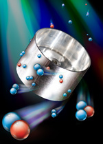
My research interests are mainly in the field of semiconductor device materials processing, and in particular plasma processing. In the semiconductor industry, plasmas are widely used to deposit and etch thin films in integrated circuits. In this regard, plasmas have played and will continue to play a major role in the continuing nano-technology revolution in electronic devices. Micro-plasmas are also increasingly finding applications in such diverse areas as high-resolution displays and bioengineering. In the plasma etching process, bombardment by positive ions normal to the wafer surface allows fine-line patterns to be transferred into thin films on the wafer surface, making it possible to fabricate integrated circuits with device dimensions of only a few hundred atoms. Such precise control of this pattern transfer process has been realized through advances in our understanding of the underlying plasma physics and chemistry, made possible through a combination of plasma experiments and modeling. Nonetheless, the lack of a more thorough understanding of the process, and especially the need for applicable diagnostic techniques, continue to hamper our ability to extend this process to ever smaller, nanometer-scale features. Our group is also interested in using plasmas in new ways. Some of our current studies include:
Nanopantography
In a joint effort with Profs. Demetre Economou and Paul Ruchhoeft (Electrical and Computer Eng.), we are exploring a new technique for massively parallel nanopatterning over large areas. A broad ion beam is directed at an array of sub-micron-diameter electrostatic lenses fabricated on the conductive substrate (e.g., doped Si wafer). By applying appropriate voltages to the lens electrodes, the "beamlets" entering the lenses are focused to spots that can be 100X smaller than the diameters of the lenses. Each lens writes identical nanofeatures on the substrate, therefore nanopantography is a parallel process, very different from focused electron beam or ion beam writing. When the substrate is tilted with respect to the ion beam axis, the focal points of the off-normal ion beamlets are scanned across the centers of the lens bottoms, making it possible to “write” any arbitrary nanopattern, as shown in the figure.

Plasma-surface interactions at a “Spinning Wall”
Some of the most important but least understood aspects of plasma processing are the interaction at the surface of the substrate (e.g. silicon wafer) and the walls of the reactor. These elusive processes have been difficult to study on real surfaces while they are exposed to the harsh plasma enviroment. We have begun studies of plasma chemistry on dynamic, reactive surfaces, using a novel spinning substrate method. In this case, the spinning wall is rapidly spun (e.g. 40,000 rpm) to bring the surface from the plasma to an analysis chamber in times of less than 1 millisecond. In the analysis chamber, mass spectrometry is used to observe short-lived species that are desorbing, while Auger electron spectroscopy is used to detect such species before they leave the surface. By varying the rotation frequency, surface reaction kinetics can be determined.

Plasma etching of new materials such as hafnium oxide
Hafnium oxide is replacing SiO2 as the dielectric layer below gate electrodes in complementary metal oxide semiconductor (CMOS) field effect transistors (FETs). We are investigating etching of this important material in boron trichloride plasmas, using a variety of diagnostic methods, including x-ray photoelectron spectroscopy (XPS). As shown below, etching in a BCl3 plasma removes the HfO2 layer, but leaves an undesirable boron residue on the underlying silicon substrate. We can successfully remove this layer with a subsequent hydrogen plasma cleaning process, as confirmed by XPS measurements such as those reproduced below.

Atmospheric pressure micro-discharges
In a joint effort with Prof. Demetre Economou, we are exploring the physics, chemistry and applications of atmospheric pressure micro-discharges. Unlike conventional high pressure plasmas, these discharges operate in a stable glow mode. We have constructed an optical emission spectroscopy microscope and a focused laser microprobe coupled with a triple grating spectrometer to obtain 3-D imaging of gas temperature, electron temperature, electron density and electric fields, and compare these quantities to model predictions. We are also starting to explore the use of micro-discharges for trace chemical sensors.
Neutral beam nano-processing
In a joint effort with Prof. Demetre Economou, new methods are being explored for nanometer scale patterning of electronic materials using energetic neutral beams.
Awards and Honors
- 2007: Graduate Program Director
- 2007: Cullen College of Engineering Senior Research Award
- 2006-2007: Session Organizer for the American Institute of Chemical Engineers Annual Symposium.
- 2005: Program Committee for the 2005 International Dry Process Symposium, Japan
- 2005: Program Committee for the 2005 International Conference on Reactive Plasmas, Japan
- 2005: Topic Organizer for the 2006 IEEE International Conference on Plasma Science
- 2004: Session Organizer for the 2004 IEEE International Conference on Plasma Science
- 2003: Plasma Prize, American Vacuum Society Plasma Science and Technology Division
- 2000-2003: Advisory Committee of The Industrial Physicist
- 1999-2001: Chair of the American Vacuum Society Plasma Science and Technology
- 1997: Fellow, American Vacuum Society
- 1995-1998: Member of the National Research Council's Plasma Science Committee
- 1995-2001: Sematech Plasma Diagnostics Process Technical Advisory Board member
- 1993: AT&T Bell Laboratories Distinguished Member of Technical Staff Award
- 1991: Tegal Corporation Thinker Award in Recognition of Pioneering Research in the Application of Optical Diagnostic Techniques to Plasma Processing
Selected Publications
-
J. Guha, V. M. Donnelly and Y-K. Pu,
“Mass and Auger Electron Spectroscopy Studies of the Interactions of Atomic and Molecular Chlorine on a Plasma Reactor Wall” J. Appl. Phys. 103, 013306
, 2008 -
L. Xu, A. Nasrullah, Z. Chen, P. Ruchhoeft, D. J. Economou and V, M. Donnelly,
“Etching of nanopatterns in silicon by nanopantography”, Appl. Phys. Letters, 92, 013124
, 2008 -
L. Xu, N. Sadeghi, V. M. Donnelly, and D. J. Economou,
“Nickel atom and ion densities in an inductively coupled plasma with an internal coil”, J. Appl. Phys. 101, 013304
, 2007 -
A. Ranjan, C. Helmbrecht, V. M. Donnelly, D. J. Economou and G. F. Franz,
“Effect of surface roughness of the neutralization grid on the energy and flux of fast neutrals and residual ions extracted from a neutral beam source”, J. Vac. Sci. Technol. B, 25, 258
, 2007 -
J. Guha, Y-K. Pu, and V. M. Donnelly,
“Auger electron spectroscopy of surfaces during exposure to gaseous discharges”, J. Vac. Sci. Technol. A, 25, 347
, 2007 -
S. J. Kang and V. M. Donnelly,
“Optical absorption and emission spectroscopy studies of ammonia-containing plasmas”, Plasma Sources Sci. Technol. 16, 265
, 2007 -
J. Guha, V. M. Donnelly and Y-K. Pu,
“Mass and Auger Electron Spectroscopy Studies of the Interactions of Atomic and Molecular Chlorine on a Plasma Reactor Wall”, J. Appl. Phys. Submitted
, 2007 -
L. Xu, A. Nasrullah, Z. Chen, P. Ruchhoeft, D. J. Economou and V, M. Donnelly,
“Etching of nanopatterns in silicon by nanopantography”, Appl. Phys. Lett., submitted
, 2007 -
C. Wang and V. M. Donnelly,
“Effectiveness of dilute H2 plasmas in removing boron from Si after etching of HfO2 films in BCl3 plasmas”, J. Vac. Sci. Technol. A, 24 41
, 2006 -
P. F. Kurunczi, J. Guha, and V. M. Donnelly,
“Plasma-Surface Reactions at a Spinning Wall”, Phys. Rev. Lett. 96, 018306
, 2006 -
Sang Ki, D. J. Economou, V. M. Donnelly,
“Particle-in-cell simulation of beam extraction through a hole in contact with plasma”, J. Phys. D (App. Phys.) 39, 3994
, 2006 -
A. Ranjan, V. M. Donnelly, D. E. Economou,
“Energy distribution and flux of fast neutrals and residual ions extracted from a neutral beam source”, J. Vac. Sci. Technol. A, 24, 1839
, 2006 -
S. G. Belostotskiy, Q. Wang, V. M. Donnelly, D. J. Economou, and N. Sadeghi,
“Three-dimensional gas temperature measurements in atmospheric pressure microdischarges using Raman scattering”, Appl. Phys. Let. 89, 251503
, 2006 -
Q. Wang, V. M. Donnelly, and D. J. Economou,
“Simulation of direct current microplasma discharge in helium at atmospheric pressure”, J. Appl. Phys., 100, 023301
, 2006 -
Q. Wang, I. Koleva, V. M Donnelly, and D. J. Economou,
“Spatially Resolved Diagnostics of an Atmospheric Pressure Direct Current Helium Microplasma”, J. Phys. D: Appl. Phys., 38, 1690
, 2005 -
C. Wang and V. M. Donnelly,
“Evaluation of the Effectiveness of H2 Plasmas in Removing Boron from Si after Etching of HfO2 Films in BCl3 Plasmas”, J. Vac. Sci. Technol. B, 23, 547
, 2005 -
L. Xu, D. J. Economou, V. M. Donnelly, and P. Ruchhoeft,
“Extraction of a Nearly Monoenergetic Ion Beam Using a Pulsed Plasma”, Appl. Phys. Lett. 87, 041502
, 2005 -
P. F. Kurunczi, J. Guha and V. M. Donnelly,
“Recombination Reactions of Oxygen Atoms on an Anodized Aluminum Plasma Reactor Wall, Studied by a Spinning Wall Method”, J. Phys. Chem. B, 109, 20989
, 2005 -
L. Xu, S. C. Vemula, M. Jain, S. K. Nam, V.M. Donnelly,
“Nanopantography: A New Method for Massively Parallel Nano-Patterning over Large Areas”, D. J. Economou and P. Ruchhoeft, Nanoletters, 5, 2563
, 2005 -
S. K. Nam, V. M. Donnelly and D. J. Economou,
“Particle-in-Cell Simulation of Ion Flow Through a Hole in Contact with Plasma”, IEEE Trans. on Plasma Sci. 33, 232
, 2005 -
V. M. Donnelly,
“Plasma Electron Temperatures and Electron Energy Distributions Measured by Trace Rare Gases Optical Emission Spectroscopy”, J. Phys. D.: Appl. Phys. 37, R217
, 2004 -
C. B. Labelle, V. M. Donnelly, G. R. Bogart, R. L. Opila, and A. Kornblit,
“Investigation of Fluorocarbon Plasma Deposition from c-C4F8 for Use as Passivation During Deep Silicon Etching” J. Vac. Sci. Technol. A, 22, 2500
, 2004 -
V. M. Donnelly,
“Optical Plasma Emission Spectroscopy of Etching Plasmas Used in Si-based Semiconductor Processing”, Plasma Sources Sci. Technol. 11, A26
, 2002 -
M. J. Schabel, V. M Donnelly, A. Kornblit, W. W. Tai,
“Determination of Electron Temperature, Fluorine Concentration, and Gas Temperature in Fluorocarbon/Argon Plasmas Using Optical Emission Spectroscopy”, J. Vac. Sci. Technol. A, 20, 555
, 2002 -
M. V. Malyshev and V. M Donnelly,
“Diagnostics of Inductively Coupled Chlorine Plasmas: Measurement of Electron and Total Positive Ion Densities”, J. Appl. Phys. 90, 1130
, 2001 -
K. Pelhos, V.M. Donnelly, A. Kornblit, M.L. Green, R.B. Van Dover, L. Manchanda, Y. Hu, M. Morris, and E. Bower,
“Etching of High-K Dielectric Zr1-xAlxOy Films in Chlorine-Containing Plasmas”, J. Vac. Sci. Technol., A 19, 1361
, 2001 -
N. C. M. Fuller, I. P. Herman, and V. M. Donnelly,
“Optical Actinometry of Cl2, Cl, Cl+, and Ar+ Densities in Inductively Coupled Cl2-Ar Plasmas”, J. Appl. Phys. 90 3182
, 2001 -
K. H. A. Bogart and V. M. Donnelly,
“Composition of Trench Sidewalls and Bottoms for SiO2-Masked Si(100) Etched in Cl2 Plasmas”, J. Appl. Phys., 87, 8351
, 2000 -
M. V. Malyshev, V. M Donnelly, S. W. Downey, J. I. Colonell, and N. Layadi,
“Diagnostic Studies of Aluminum Etching in an Inductively-Coupled Plasma System: Determination of Electron Temperatures and Connections to Plasma-Induced Damage”, J. Vac. Sci. Technol. A. 18, 849
, 2000 -
S. Samukawa, K. Noguchi, J. I. Colonell, K. H. A. Bogart, M. V. Malyshev, and V. M Donnelly,
“Reduction of Plasma Induced Damage in an Inductively Coupled Plasma Using Pulsed Source Power”, J. Vac. Sci. Technol. B, 18, 834
, 2000 -
M. V. Malyshev and V. M. Donnelly,
“Dynamics of Inductively-Coupled Pulsed Chlorine Plasmas in the Presence of Continuous Substrate Bias”, Plasma Sources Sci. Technol. 9, 353
, 2000 -
S. Samukawa, V. M. Donnelly, and M. V. Malyshev,
“Effects of Discharge Frequency in Plasma Etching and Ultrahigh Frequency Plasma Source for High-Performance Etching for ULSI”, Jpn. J. Appl. Phys., 39, 1583
, 2000 -
M. V. Malyshev, N. C. M. Fuller, K. H. A. Bogart, V. M. Donnelly, and I. P. Herman,
“Diagnostics of Inductively Coupled Chlorine Plasmas: Measurement of Cl2+ and Cl+ Densities”, J. Appl. Phys. 88, 2246
, 2000 -
M. V. Malyshev and V. M Donnelly,
“Diagnostics of Chlorine Inductively Coupled Plasmas: Measurement of Electron Temperatures and Electron Energy Distribution Functions”, J. Appl. Phys, 87, 1642
, 2000 -
M. V. Malyshev and V. M Donnelly,
“Diagnostics of Inductively Coupled Chlorine Plasmas: Measurement of Cl2 and Cl Number Densities”, J. Appl. Phys. 88, 6207
, 2000 -
V. M Donnelly and M. V. Malyshev,
“Diagnostics of Inductively Coupled Chlorine Plasmas: Measurements of the Neutral Gas Temperature”, Appl. Phys. Lett., 77, 2467
, 2000 -
N.C.M. Fuller, M.V. Malyshev, V.M.Donnelly, and I. P. Herman,
“Characterization of Transformer Coupled Oxygen Plasmas by Trace Rare Gases-Optical Emission Spectroscopy and Langmuir Probe Analysis”, Plasma Sources Sci. Technol. 9, 116
, 2000 -
S. Samukawa, K. Noguchi, J. I. Colonell, K. H. A. Bogart, M. V. Malyshev, and V. M Donnelly,
“Reduction of Plasma Induced Damage in an Inductively Coupled Plasma Using Pulsed Source Power”, J. Vac. Sci. Technol. B, 18, 834
, 2000 -
V. M Donnelly, M. V. Malyshev, N. C. M. Fuller, K. H. A. Bogart, and I. P. Herman,
“Determination of Concentrations and Temperatures of Charged and Neutral Species in Chlorine Inductively-Coupled Plasmas”, Proceedings of the Symposium on Dry Process, Tokyo
, 2000

